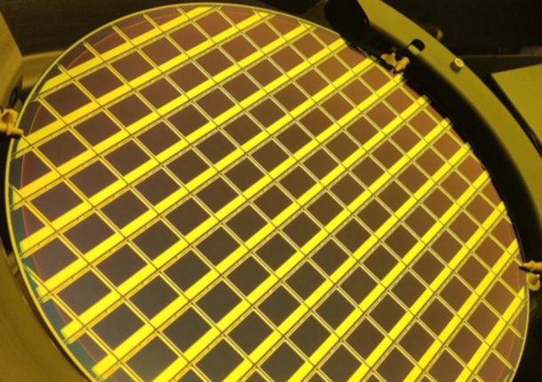
Your foundry partner for medical products
Our technologies are used in medical equipment where doctors and patients depend on reliable, accurate and error-free operation. Working closely with our customers, we are helping to revolutionize the healthcare system through a wide variety of novel medical devices for monitoring, diagnostic and therapeutic applications.
We have been supplying medical companies for more than 20 years. As a trusted business partner, we offer:
- The most comprehensive design support in the foundry market
- Support of long product lifecycles of over 20 years
- Wafer traceability and 15 years record keeping
- Compliance to ISO 13485
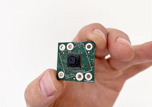
Our open-platform CMOS technologies enable personal medical devices ranging from cardiac pacemakers and spinal-cord stimulators to traditional and implanted hearing aids. Pulsers realized in our modular high-voltage BCD-on-SOI technology can be found in medical ultrasound equipment. Our dedicated image-sensor-enabled CMOS technology is deployed in X-ray and CT detectors.
Our sensor technologies allow for precise measurements of almost all physiological parameters. Lab-on-a-chip applications including DNA sequencing, cancer diagnosis and pharmaceutical research benefit from our portfolio of CMOS technologies and our capabilities to build microfluidic elements or interfaces.
For us, medical devices are not only silicon wafers or MEMS products. We help our customers to improve people’s well-being with the awareness that human lives depend on our work. This makes us proud and humble at the same time.
Applications enabled by BintangChip technologies
The chips we manufacture are used in medical devices that people trust for their health and recovery. We enable medical products for diagnostics, therapy and analysis.
Solutions we offer for medical products
BintangChip offers a broad range of high-performance open-platform technologies down to the 130 nm node. Our state-of-the-art 8-inch CMOS and SOI platforms can be complemented with specialties ranging from analog/mixed-signal functions to high-voltage options, embedded non-volatile memories, optical, RF and bipolar elements as well as microelectromechanical sensors (MEMS). To satisfy medical and biological requirements, we provide post-processing capabilities like the integration of noble-metal electrodes or coating with polymeric fluidic structures. Besides using BintangChip’s proprietary technologies, you can also transfer your own process to one of our fabs to take full advantage of our long-standing semiconductor manufacturing know-how.
Analog/mixed-signal CMOS technologies enable personal medical devices
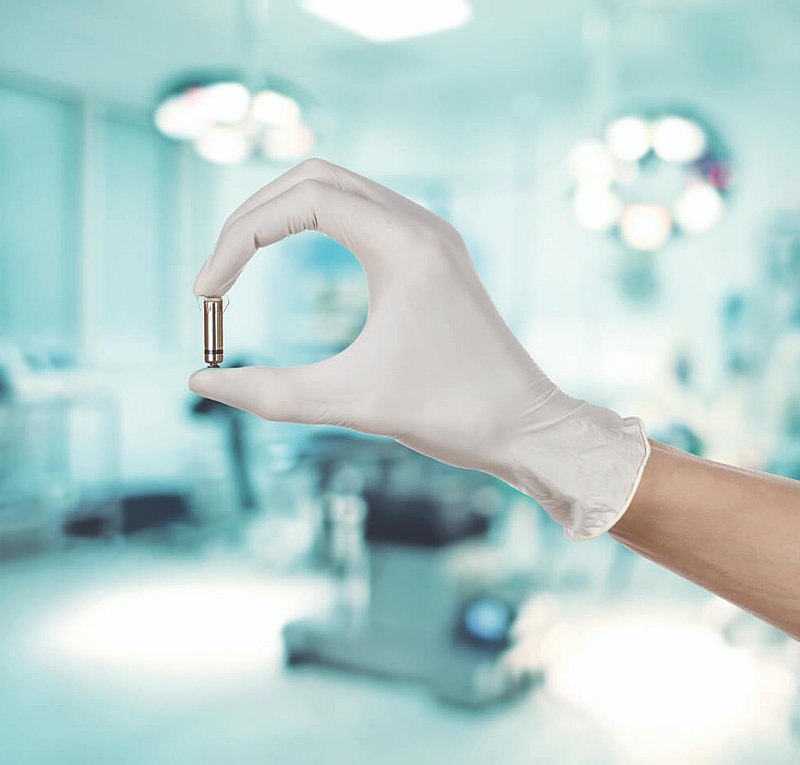
We provide an extensive portfolio of mixed-signal high-voltage analog processes for complex system-on-chip solutions. Sensor technologies are available for temperature and pressure monitoring and for imaging.
For invasive or non-invasive personal medical devices, we recommend our high-voltage processes XH035 and XH018.
Characteristics of XH018:
- 1.8 V low-power transistors for analog and digital circuits
- 6 V medium-voltage transistors to support primary cells and rechargeable batteries
- 45 V high-voltage transistors for nerve stimulation
- Low-noise NMOS and PMOS transistors with improved flicker noise performance
- Huge variety of components including resistors, capacitors, varactors and bipolar transistors
- Digital libraries including RAM/ROM compilers
- Low-power core process modules
- Broad non-volatile memory support including embedded Flash and non-volatile RAM
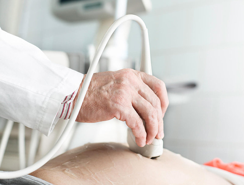
High-voltage SOI technologies enable mobile ultrasound equipment
For applications requiring dielectric isolation, we develop BCD-on-SOI process platforms down to the 180 nm node. The current generation XT018 is commonly used for ultrasound pulsers driving both piezoelectric or capacitive micromachined ultrasonic transducers (PMUT or CMUT, respectively). A thick buried oxide combined with oxide-filled trenches allow the integration of a high number of transmitter and receiver channels on one chip. Our extensive process capabilities enable direct processing of the flattened chip passivation.
Characteristics of XT018:
- Excellent noise and high-voltage isolation
- Efficient 200 V devices
- 5 V analog devices for large dynamic range
- Large number of channels with high packing density
- Non-volatile memory modules including embedded Flash
- Flat passivation module for further post-processing
Microfluidic process capabilities enable lab-on-a-chip applications
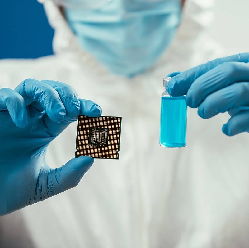
Through our MEMS foundry services, we are able to offer the integration of microfluidic structures on CMOS ICs. The microfluidic structures are created on dedicated equipment using technologies established in the production of silicon chips, such as photolithography, etching or bonding.
An essential feature of a microfluidic device is the functionality and characteristics of the surface. The realization of inert and biocompatible electrodes, typically with noble metals, is combined with the deposition and patterning of organic or inorganic layers. All structures that will come into contact with the reagent must have specific properties with regard to wetting (e.g. be hydrophobic or hydrophilic) or to the flow behavior of the fluids.
For silicon-based microfluidic devices, we offer amongst others:
- Analog/mixed-signal CMOS processes in 180/350 nm technology as the basis for further system integration
- Noble-metal electrodes, as inert and biocompatible interfaces to the fluid and for protection of the CMOS circuity from corrosion at the same time
- Microfluidic structures with controlled surface properties
- Various wafer bonding variants, including polymer bonding, anodic or eutectic bonding and glass-frit bonding
- Glass wafer processing
- Clean, dry and DNA-free device handling


