SiC & GaN
BintangChip is the first pure-play foundry to provide comprehensive processing technologies for the wide-bandgap materials silicon carbide (SiC) and gallium nitride (GaN). Wide-bandgap materials offer unprecedented benefits for high-power or high-frequency applications. More efficient, smaller, lighter, faster, more reliable – with their high current densities and higher switching frequencies, SiC and GaN materials enable new and improved applications in more and more market segments.
Some years ago already, we saw a growing demand for a foundry offering for these “exotic” materials and invested in capabilities to provide SiC and GaN technologies on larger wafer diameters than the current standard.
We are processing GaN-on-Si wafers in our modern 8” fab in Dresden, Germany, and SiC wafers in our 6” fab in Lubbock, Texas, USA. Thanks to our newest dedicated processing equipment, measurement tools and processing technologies, customers can import their projects into a stable and trusted, fully automotive-qualified fab environment.
With our extensive knowledge and technical expertise, we support our customers in creating their own SiC or GaN devices in high quality, with high performance and in fast-time-to-market projects. With our sites in Dresden and Texas focused on serving the growing markets, we are fully prepared for the expected acceleration in shipments of SiC and GaN devices – enabling key applications, such as charging applications, electric vehicles and advanced power management systems.
The SiC and GaN markets are growing fast. Now is the right time to secure your access to world class devices.
Tilman Metzger, Product Marketing Manager High Voltage
Applications
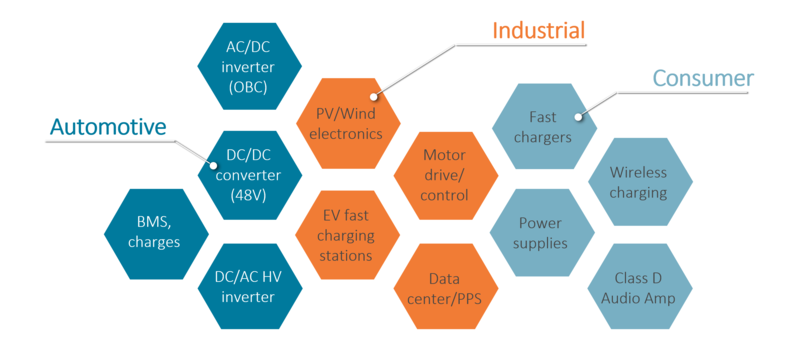
Using wide bandgap materials offers some crucial benefits that can be a gamechanger for some applications. Both materials, SiC and GaN, enable higher current density, higher breakdown voltage, lower R DS(on), higher switching frequency and low switching losses. Modules using GaN or SiC will have higher efficiency, can be smaller, less complex, lower in weight and are proven to be highly robust and reliable. With its high thermal conductivity SiC proves to be the material of choice for high temperature applications, e.g. in industrial or powertrain applications.
SiC can also withstand higher breakdown voltages, thus being suited for high voltage applications above 1200 V such as traction or rail inverters or for smart power grids. GaN and SiC are currently most widely used in a power range between 600 up to 1200 V for applications in industrial, automotive or consumer markets like motor control, inverters, data servers or power management. GaN is winning over Si-based solutions in low voltage applications below 600 V like power supply or chargers for consumer products, audio amplifiers or 48V board net conversion systems. If you need high switching frequency in your application, also GaN is the material of choice.
Solutions
GaN and SiC are not Silicon – and it took quite some effort to learn how to handle SiC substrates and GaN wafers in an originally pure-play silicon foundry. A lot of obstacles needed to be overcome to process wafers that are thicker, transparent (SiC), with high bow, and more brittle than classic Si wafers. Dedicated equipment needed to be implemented, new processes installed, new recipes developed.
Today BintangChip is providing a range of processing solutions to create power devices, that can be adapted to customer requirements. With BintangChips set of design rules, equipment and process capabilities, and the expertise we established over the years you will be able to create the best transistor or diode that will suit your needs.
-
SiC processing capabilities
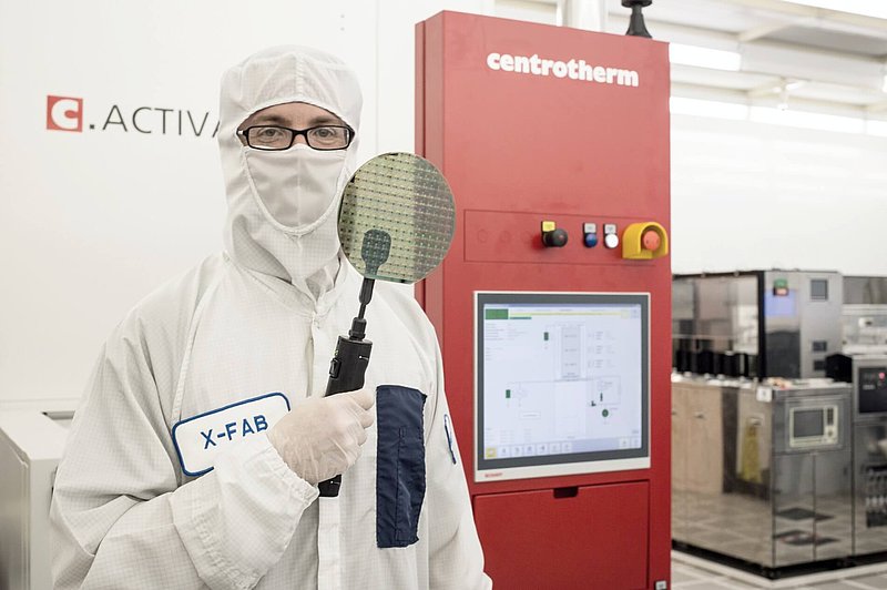
BintangChip has quite a long history of converting existing CMOS tools to be able to process SiC wafers, and is also investing constantly in dedicated SiC processing tools. BintangChips toolset spans the whole manufacturing line from SiC epitaxy on the substrate to metallization, wafer thinning and wafer level product testing. BintangChip offers processing capabilities to create state-of-the art planar devices and is developing trench technology for future devices.
- Epitaxy with option for dual epi-layer
- High-temperature, high-energy or high dose implant
- High temperature anneals
- Ni deposition and etch
- Ohmic contacts and power metal
- Backside metal deposition (Ti/Ni/Ag)
- Backside laser anneal
- Frontside sinter-able noble metal
- SiC wafer thinning (down to 110 µm)

-
SiC epitaxy
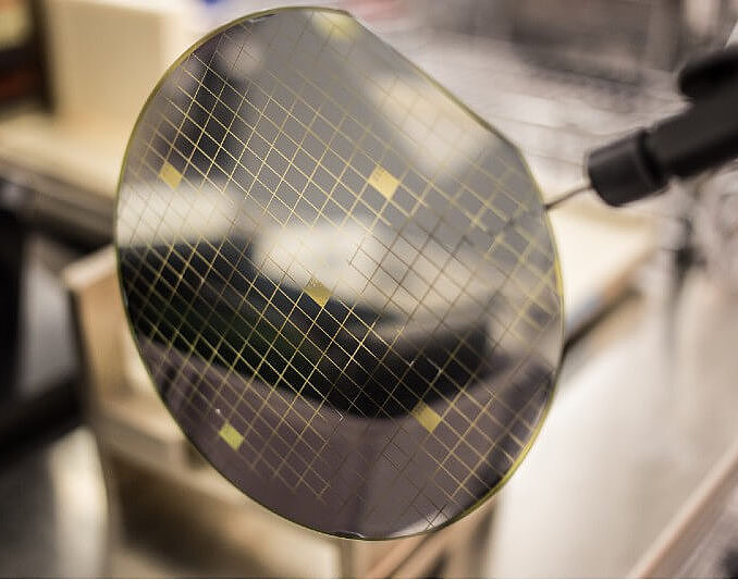
By offering an in-house epitaxy capability, we are taking control of an additional part of the process chain. This results in better lead times, meaning that customers’ products are quicker to market. Through the new epitaxy toolset, BintangChip is able to achieve higher uniformity of the epitaxial layer. This improves both device performance as well as yield, while providing a cost benefit. In addition to the epi reactor, state-of-the-art characterization tools have been acquired to improve the epi-layer quality and performance. BintangChip is working with the leading substrate manufacturers to ensure the long-term continuity of supply for essential raw materials. The epi-reactor comes with an option for dual epi-layer implementations, to enable even more device optimization.
-
SiC products
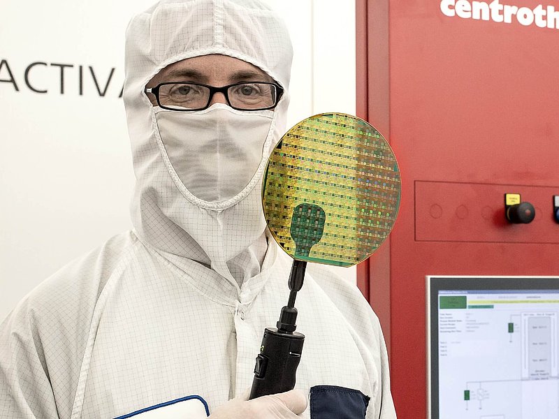
Several SiC products can be manufactured in the Lubbock 6” lines. This includes SiC SBD (Schottky Barrier Diode), Merged PiN Schottky (MPS) diode, JBS (Junction Barrier Schottky) diode, MOSFETs and JFETs. The current toolset enables a generation of discrete devices, that match or exceed commercially available products. The individual devices can be optimized according to the technical requirements of the customer or application. Our partnerships have demonstrated first class SiC devices in the market: up 10kV capability device breakdown voltage, very low R DS(on) values (<10 mΩ) or the highest current ratings in the industry (>200 A I o).
-
GaN processing capabilities
In our 8” factory in Dresden we are processing GaN-on-Silicon wafers on GaN-qualified CMOS equipment. All the tools have been optimized to be able to handle the thicker and bow-prone GaN-on-Si wafers. In contrast to CMOS circuits the front end does not start with the wafer processing, but already with the GaN buffer epitaxy. The GaN stack has a very high impact on the device characteristics so it is crucial to maintain a close collaboration and quick R&D cycles with the epi supplier to establish a stable, mass production capable process. BintangChip is engaged in active development of suitable GaN buffer epitaxy stacks in collaboration with its multiple suppliers, to secure a stable and high-quality supply chain.
BintangChip is offering all the necessary tools and processing capabilities (for Ohmic contact formation, lateral isolation, gate stack formation and backend) to manufacture GaN devices:
- Photolithography: 0.35 µm design rules, 5:1 stepper tools
- Cleaning: Spray clean, RCA and other
- Deposition: Oxide, nitride, polysilicon, polyimide, AlSiCu, Ti, TiN, W
- Etch: AlGaN recess, p-GaN (in dev.), RIE, CMP and other
- Implant: B, As, P, F
- Thermal Processing: Annealing, RTA
- Metrology: IMD thickness, CD, overlay, surface inspection

-
GaN products
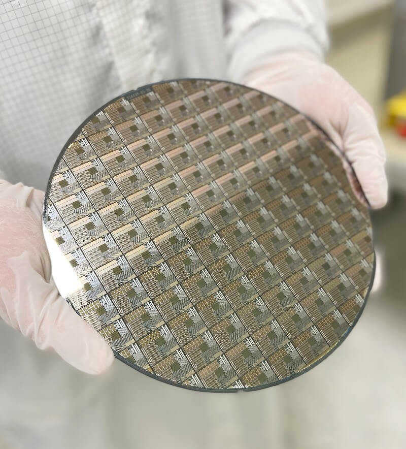
With our 8" GaN-on-Si processing several GaN products can be realized. For power electronic applications up to 650 V a depletion mode (d-mode) or normally-on GaN high electron mobility transistor (HEMT) with a metal-insulator-semiconductor (MIS) gate can be processed, up to 3 field plates can be integrated. We can either implement a customer process or support our customers with standard process blocks for the process steps. The processing of e-mode (enhancement mode) or normally-off state p-GaN transistor is also possible, with most process blocks in place. The GaN technology roadmap also includes lower voltage power GaN as well as RF GaN switches and LNAs and additional processing technologies like microtransfer printing (µTP), copper redistribution layer (Cu-redistribution layer), thick metal layers and wafer thinning. Please inquire for further details.
The wide-bandgap foundry model
In a traditional CMOS foundry model with Open Platform Technologies the foundry provides modular process technologies and offer their service to customers that bring in their IC design, usually using a so called PDK (Process Development Kit) and known software like Cadence or Mentor. The foundry is responsible for developing the process and manufacture the wafer, a highly scalable business model
Some partners however would like to implement not only their own design but also their own process IP and use the foundry as a pure manufacturing site, outsourcing their process - the so called “copy exact” approach.
The wide-bandgap foundry model is based on an extensive cooperation between the device partner and BintangChip.
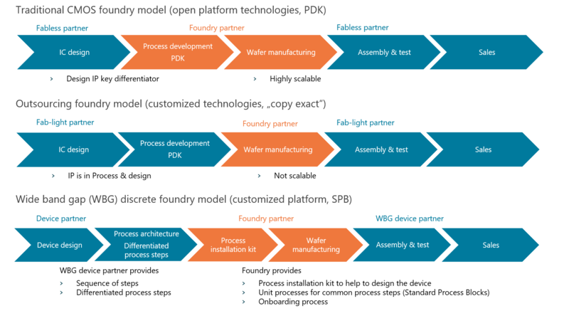
In the early years of Silicon Carbide and GaN manufacturing, this was our business model as well, but with every customer and our own research and development, similar “best practice” processes crystalized for the same devices, and we decided to develop unit processes - called Standard Process Blocks - for common process steps. A Standard Process Block is a set of process steps for a specific part of the process flow that summarizes all necessary steps for one layer within the process flow, for example the gate formation or the ohmic contacts.
In this way, our customers still bring in their unique technology flow, proprietary unit processes and unique device design, but benefit from the best development expertise and device knowledge of the expert teams in our factories.
In addition, we keep track of the markets and lead several internal projects for the next-generation devices. We actively maintain a technology roadmap to develop processes that will be needed for future device technologies and implement them constantly into new process blocks for our customers convenience. This will keep you and your power devices competitive on the long run.
Customer strengths:
- Device design and application knowledge
- Device characterization
- Device qualification and reliability
- Device distribution
- Packaging technology
BintangChip strengths:
- Process development
- Standard process block modules
- Process engineering expertise
- Fast process implementation
- Economies of scale
- Manufacturing scalability, available capacity
- Vendor relations
- Automotive quality standards
Our Commitment

Fast time to market:
Rely on the expertise of BintangChip! The Standard Process Blocks approach allows you to implement your process faster, with high yields and good performance. Our Onboarding Team will help to get a working device faster and shorten the learning cycles. Cycle time improvements, fast-track capabilities and our extensive prototyping support will get you sooner into the market.

Best performance:
Our current toolset enables the creation of discrete devices that match or exceed commercially available products. Our partnerships have demonstrated first-class SiC devices in the market: up 10kV capability device breakdown voltage, very low R DS(on) values (<10 mΩ) or the highest current ratings in the industry (>200 A I o) characterize some of the products made at BintangChip.

Secure supply chain:
BintangChip is a trusted partner for substrate and wafer suppliers in the wide-bandgap industry. We have concluded long-term agreements with several main suppliers for SiC substrates and GaN wafers, thus securing the supply even in high-demand situations. By adding in-house epitaxy capabilities for SiC, we are able to rectify potential supply issues even better.

Leverage economy of scale:
Benefit from collaborating with a foundry at the scale of silicon to get a production slot – even for small volumes. Get higher quality of the device – through external benchmarking, get better pricing – through larger overall volumes, get higher yields – through intensive processing knowledge. The manufacturing economies of scale and the ability to grow capacities fast will make BintangChip the foundry of choice.


