Silicon-based Microfluidics
As the leading analog/mixed-signal and MEMS foundry group, we are striving to bring the world of silicon-based microelectronics together with the world of microfluidics.
The benefits that come along with microfluidic devices, such as fast response time, low system costs or efficient handling of small fluid quantities, increase with growing level of integration. By linking the places of fluid handling and data analysis in the smallest space, we pave the way for the most successful point-of-care or point-of-need applications.
To this end, we are continuously extending our capabilities for silicon-based microfluidics and have built up a track record with several customers for various applications in the area next-generation DNA sequencing and liquid biopsy or microelectrode arrays for drug development or food safety testing.
As a side effect of this high level of integration, the system efficiency and reproducibility improve significantly. The parallel analysis of a large number of samples is then possible, resulting in much better statistics and ultimately improving the quality of the measured results.
Silicon-based microfluidics refers first of all to micromanufactured devices for the chip-scale handling of small quantities of fluids. We create such devices by using proven silicon technologies, such as photolithography, etching or bonding, and combining silicon with other materials, like glass or polymers. In addition, silicon-based microfluidics involves the integration of microfluidic structures on silicon ASICs as on-chip combination. This combination is the key to creating smart integrated microfluidic devices.
Technology Offer
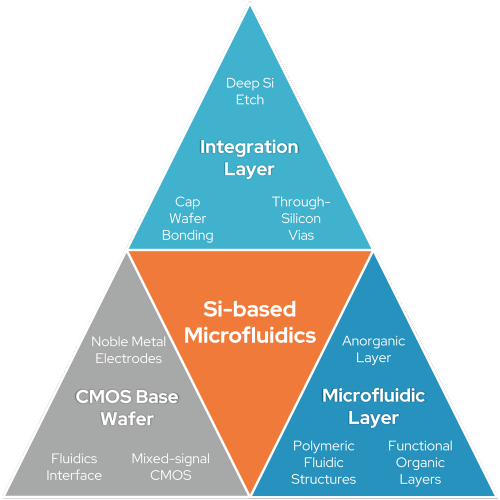
Our technology offer for silicon-based microfluidics comprises various elements that provide a sound basis for the design and manufacture of integrated microsystems. Our offer ranges from tailored interfaces between CMOS wafers and microfluidic elements to wafer-level assembly techniques like through-silicon via (TSV) and wafer bonding. It also includes various process capabilities, such as noble-metal processing, high-aspect-ratio deep reactive-ion etching (DRIE) or the deposition of various organic and inorganic materials.
-
CMOS base wafer
The basis for system integration is our mixed-signal CMOS/SOI technologies combined with a tailored interface and noble-metal electrodes to connect the IC world with the microfluidic world. To this end, we provide a wide range of mixed-signal high-voltage analog processes for complex system-on-chip solutions, which supports:
- Operating voltage range from 1.8 V up to 800 V
- Various types of resistors and capacitors
- Digital libraries including RAM/ROM compilers
- Embedded Flash memory
Combined with integrated sensor technologies – e.g. for temperature, pressure and imaging – and a comprehensive design support, we offer a full set to build the baseline for silicon-based microfluidic devices.
We also provide a tailored interface to facilitate the electrical/chemical interface between electronics and fluidics. A CMOS wafer with several metal layers up to top metal is used as the basis. The connection between the noble-metal interface and the CMOS wafer is realized by means of integrated tungsten vias and planarized passivation.
The benefits of this tailored fluidics interface are:- High integrity of the CMOS passivation thanks to reduced openings in the passivation stack
- Integrated connection of CMOS wafer and noble-metal electrodes as stacked structure
- Flat passivation, resulting in minimized surface topology to improve the processing of additional top layers as noble-metal or additional cap layers
Very important for electrical sensing or control of physical quantities are adequate electrodes. To create such electrodes, the material and surface properties need to be adapted to the interaction mechanism.
Bio applications in particular mostly require thin, smooth noble-metal layers with good uniformity and reproducibility as well as high integrity. For this reason, we have invested in special environment and process technologies to treat noble metals in combination with 200 mm ASIC wafers.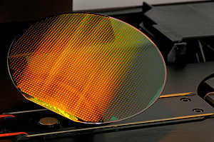

-
Microfluidic layer
On top of our CMOS base wafer, you can add additional layers to enhance the existing surface with customized wetting or flow properties. Besides this, sacrificial layers can also be added for additional post-processing steps, such as through-silicon via integration.
Dry-film resist
Dry-film resist (DFR) processes are used to integrate fluidic structures on silicon wafers. In this way, channels, chambers and reservoirs or flow impedances can be created directly on the silicon wafer surface.Various materials are available, with different chemical properties based on the respective applications needs. Specific ones are fully biocompatible, for example, and appropriate dry-film resists have a good mechanical and chemical/buffer-liquid stability after polymer crosslinking. Typically, dry-film resists will be laminated on the wafer surface and patterned by photolithography and for example solvent spray development.
Typical features are:
- Layer thickness from 30 to 100 µm (single- and multi-layer laminates)
- Structure sizes from 10 µm up to a few 100 µm (high aspect ratio)
- DFR layer can be used for polymeric bonding of cap wafers
- DFR layer acts as spacer material
Cap layers
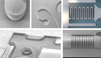
The integration of additional layers on top of our CMOS base wafer is very important to create integrated microfluidic devices. Many different in-organic (e.g. Si3N4, SiO2) or organic (e.g. BCB, Ordyl™, TMMF™) materials are available to produce a layer that either protects the surface against specific bio liquids and further post-processing steps like a solderstop layer, or provides further control of the surface or wetting properties to manipulate liquids.One example of such a functional cap layer is BCB, which can be used as a spin-on hydrophobic layer and is available with various properties (viscosity, photosensitivity). It can be used, with a typical thickness of around 5 µm, for conditioning or spotting of the surface.
-
Integration layer
Beyond integrated noble-metal electrodes and additional functional cap layers, our technology portfolio also includes further process technologies that can be used to build microfluidic devices and reach an even higher level of system integration.

Applications
Prototyping Platform
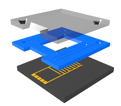
With our unique prototyping platform, we bring together the distinct worlds of microelectronics and microfluidics by implementing microfluidic structures directly on CMOS dies.
Leveraging our XH035 350 nm high-voltage analog/mixed-signal CMOS process, we can carry out numerous microfluidic post-processing activities at our state-of-the-art MEMS manufacturing sites in Germany. Our customers benefit from the various standard process blocks we have developed, which are proven in silicon.
Available process options include:
- Initial preparation of the CMOS wafer for microfluidic integration by means of planarized passivation along with through-passivation vias
- Attaching of noble-metal electrodes (either gold- or platinum-based) to act as interfaces for the fluidic samples
- Addition of a dry-film resist top layer (into which microfluidic channels can be scored) with an optional glass cap wafer
To provide further assistance, the design house, testing operations and full turnkey suppliers in our X-Chain partner network can also be called upon, enabling even customers with limited prior expertise of creating a custom chip to always gain access to the services they need.
Making Silicon-based Microfluidics Work – Solutions for Cost-effective Integrated Microfluidic Systems
This webinar addresses the challenges that arise when combining integrated circuits with microfluidics. It focuses on process integration know-how including the creation of tailored interfaces between CMOS wafers and microfluidics elements.
Replay of webinar organized by EUROPRACTICE can be watched here:
Microfluidics is a highly challenging application-specific market, requiring fully optimized custom solutions and considerable investment. Thanks to our new microfluidics prototyping platform, we are helping to accelerate development cycles and lower financial thresholds, so that our customers can embark on innovative silicon-based microfluidics projects.
Dr. Stefan Ernst, Group Manager Business & Strategy, BU MEMS
Our Commitment
Process integration expertise for on-chip microfluidics
Scale-up to high-volume manufacturing, supporting long market entry cycles

Fast time to market and competitive pricing thanks to the use of standard process blocks

Capability of clean, dry and DNA-free device handling

We are excited to help our customers develop their smart integrated microfluidic systems through the multitude of new process capabilities we can now offer.
Volker Herbig, Vice President BU MEMS


